| ALS-600(S) T/R Relay Replacement |
|
A local fellow Amateur Radio Operator has shown interest in the MJF - Ameritron ALS-600S Linear Amplifier; and, he mentioned about reading various cw experiences with respect to the Amplifiers Transmit / Receive, T/R, Relay.
A quick Internet search revealed that a Mr. Salas, AD5X, has created a Circuit [File: 'QSKals500als600RevA.pdf'] - replacing the individual T/R Relay with two (2) miniature Relays, and a Diode. |
|
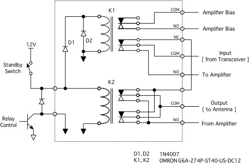
After viewing the above AD5X Documents Schematic, and ALS-600(S) Schematic Diagram, it appears that RL2 is protected by an external reversed Silicon Diode; however, RL1 is not protected - from its collapsing Magnetic Field. Also, it seems that AD5X's Printed Circuit Board, PCB, is double sided.
|
I decided to create a new Schematic Diagram, and attempt several single sided variations of the Printed Circuit Board design. Traces are on the Solder Side of PCB.
It is assumed that a 16 Pin DIP Socket - with Pins 2, 3, 5, 7, 10, 12, 14, and 15 removed, is used.
|
|
Schematic Diagram 01: [Note: K1 is the upper Relay - connected to the Amp Bias, RF Input, Amplifier Input, and Amp Bias Pads]
|
|
|
Several Printed Circuit Board designs.
Note:
Since I do not have an ALS-600(S) available; nor the dimensions of the T/R Relay - the PCB Designs provided below are suggestions only.
|
|
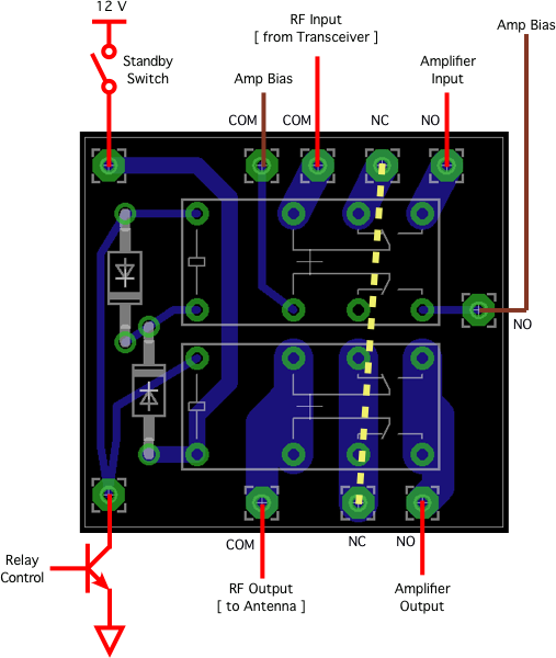
Design 01: [Note: K1 is the upper Relay - connected to the Amp Bias, RF Input, Amplifier Input, and Amp Bias Pads]
|
|
Above is a near match to the Ad5X PCB Layout, with the additional Diode.
|
|
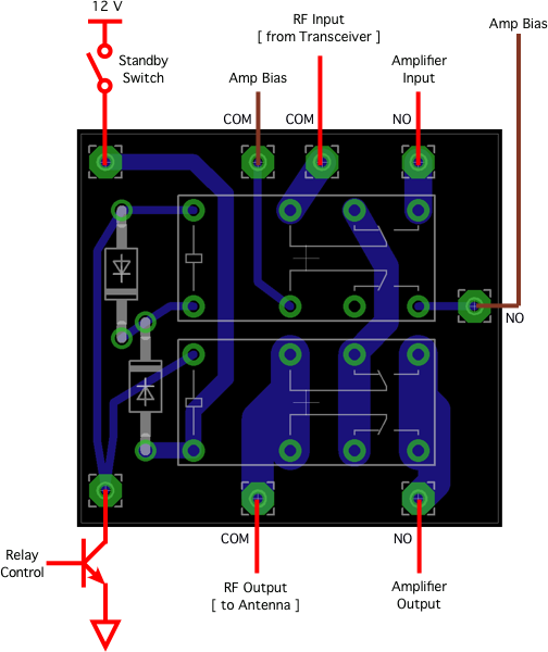
Design 02: [Note: K1 is the upper Relay - connected to the Amp Bias, RF Input, Amplifier Input, and Amp Bias Pads]
|
|
Above is a PCB Layout, where a thick insulated Wire Lead, shown as a Yellow dash Line, jumpers the respective two (2) Relays Normally Closed Contact Pads from beneath the PCB.
|
|
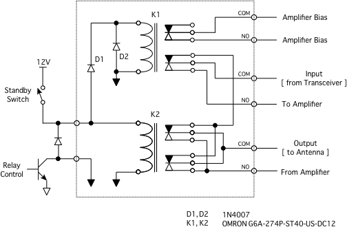
Schematic Diagram 02: [Note: K1 is the upper Relay - connected to the Amp Bias, RF Input, Amplifier Input, and Amp Bias Pads]
|
|
In this Schematic Diagram K1's Lower Normally Closed Contact is directly connected to the Normally Closed Contacts of K2. This minimizes, by two (2), the number of Jumper Leads from the original T/R Relay Base to the Relay Replacement PCB.
|
|
Design 03: [Note: K1 is the upper Relay - connected to the Amp Bias, RF Input, Amplifier Input, and Amp Bias Pads]
|
|
Above, the single Normally Closed Trace of K1 navigates between Pins 6 and 8 of K1, to Pins 9 and 11 of K2.
|
|
Design 04: [Note: K1 is the upper Relay - connected to the Amp Bias, RF Input, Amplifier Input, and Amp Bias Pads]
|
|
Above, Pin 6 of K1's DIP Socket is removed, or its Pin is cut or bent up - since no Hole to the Solder Side is provided; thus, allowing for a thick straight Trace from K1 Pin 11 to Pins 11 and 6 of K2.
|
|
| Return to KF3G |
|
Created 18.11.2015, Modified: 17.01.2015
©2008 - 2099, Alle Rechte vorbehalten, SJWL |